SPIE panel: edge placement error is now a system-level lithography problem
At the SPIE Photomask Technology + EUVL conference, experts from ASML, Micron, Applied Materials, Carl Zeiss SMT and Tekscend argued that edge placement error (EPE) is no longer a narrow lithography metric but a system-level measure of design-to-silicon fidelity. Reducing EPE requires coordinated work across OPC, masks, scanners, resist, etch and metrology, with AI paired with physics and validation.
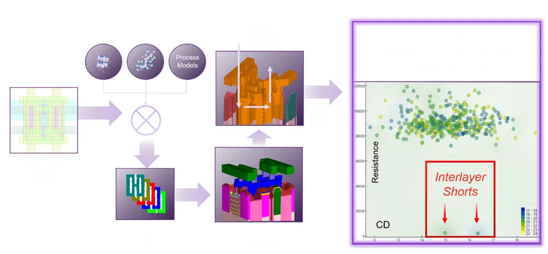
- EPE spans mask, scanner, resist, etch, metrology and OPC
- 58% of audience poll respondents expect OPC to drive EPE reduction
- AI must be explainable, physics-bounded and validated for production
- EDA should link EPE to power, performance, area, cost and yield
Read next
Hardware