US works on new EUV lithography materials for higher-density chips
Researchers in the US, together with industry partners, are developing new EUV lithography materials to print circuit patterns 50,000 times thinner than a human hair and enable smaller, denser chips. Berkeley Lab's Center for X-Ray Optics, a EUV pioneer since the late 1990s, plays a central role.
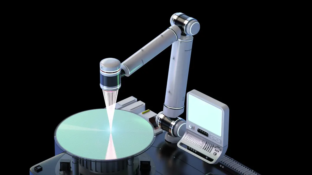
- EUV lithography prints patterns 50,000 times thinner than a human hair
- Berkeley Lab's CXRO has advanced EUV since the late 1990s with SEMATECH
- Today's best microchips pack more than 100 billion transistors
- Goal is smaller chips with even more transistors per die
Read next
Hardware