Researchers control 2D semiconductor growth for future chips
Researchers from KAIST and startup TDS Innovation demonstrated an EF-SCN process that suppresses random crystal nucleation in 2D semiconductors, allowing growth only at the geometric center of each patterned region. The method yielded single crystals at 397 of 400 sites on a 2 cm substrate (99.3%), and MoS₂ transistors showed higher charge-carrier mobility. Commercial use of 2D semiconductors is targeted for around 2030.
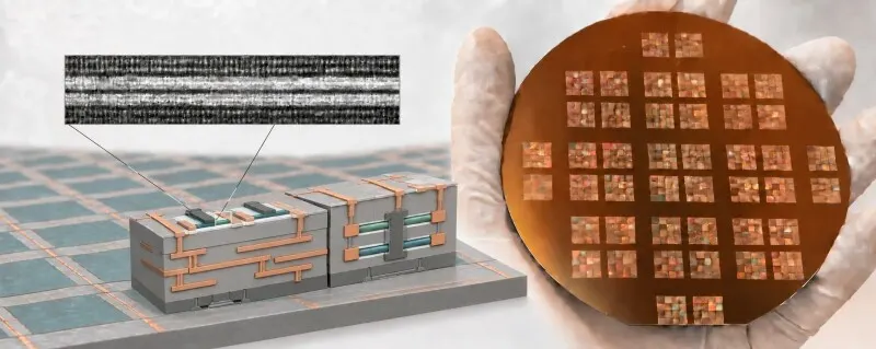
- EF-SCN uses an oxygen etching flux to suppress nucleation outside the region's center
- Single-crystal yield reached 397 of 400 sites on a 2 cm substrate (99.3%)
- MoS₂ transistors showed higher charge-carrier mobility than previously reported
- Commercial use of 2D semiconductors is targeted for around 2030
Read next
Hardware