IBM and Siemens Collaborate on Nanostack Transistor Architecture
IBM and Siemens announced joint research to advance IBM's nanostack architecture, a 3D nanosheet-based transistor design unveiled earlier this year. At the 7 angstrom node, it packs nearly 100 billion transistors into a fingernail-sized area.
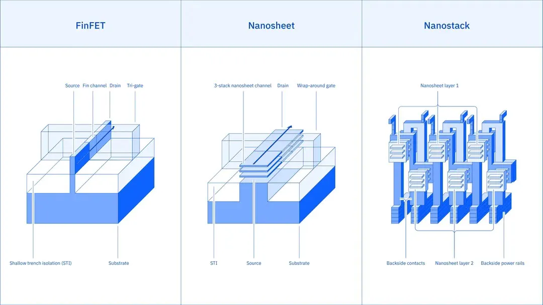
- Nanostack is the first known 3D nanosheet design with vertically stacked, staggered transistors
- Density: nearly 100 billion transistors in a fingernail-sized area at the 7 angstrom node
- Siemens brings expertise in EDA, process simulation and lithography optimization
- Different material combinations per layer allow independent transistor optimization
Read next
Science